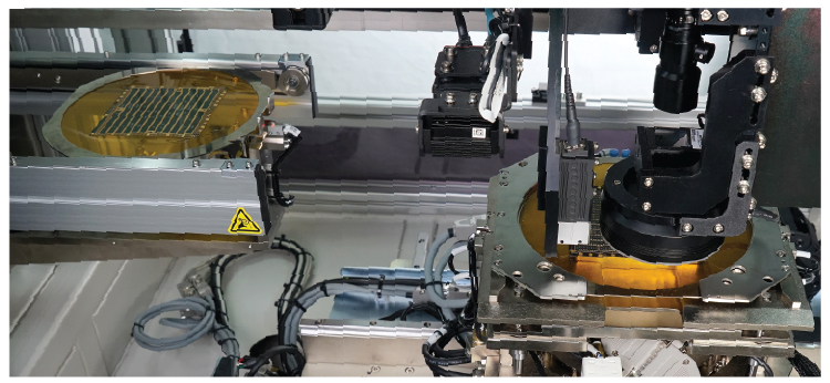
Wafer Wire Bond Inspection Machine | WI300
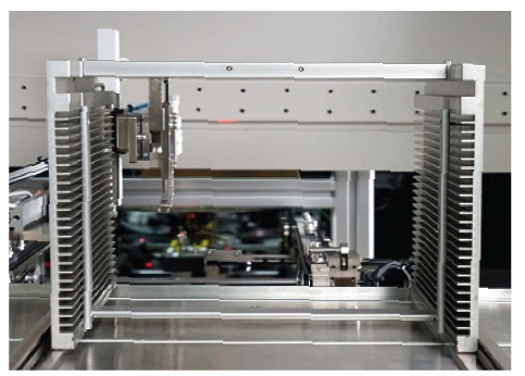
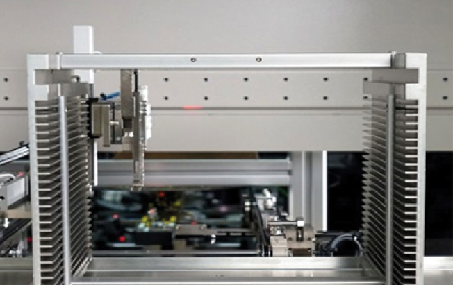
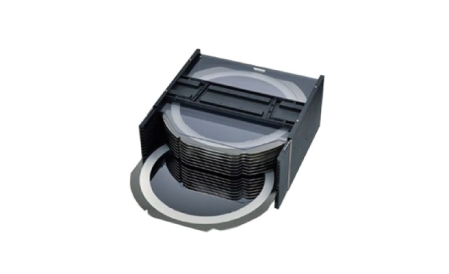
Wafer Magazine
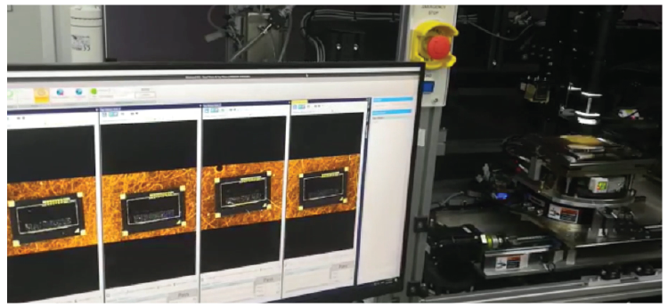
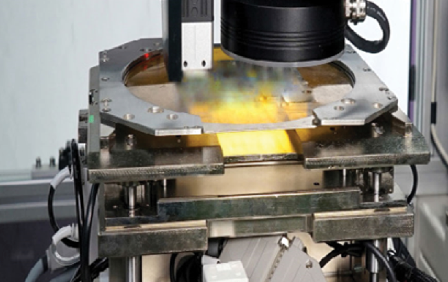
Top Vision Inspection
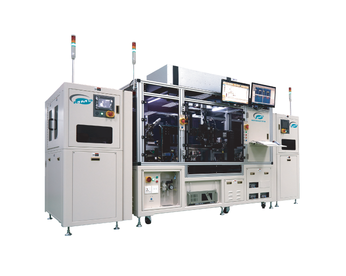
Combining high-resolution AOI, intelligent wafer mapping, and AI-ready defect analysis, the WI300 Automated Wire Bond Inspection Machine delivers 100% automated inspection of wire bonds and wafer-level defects, helping manufacturers achieve higher yields and greater reliability.
Supporting wafers from 4″ to 12″, the wafer die and wire bond inspection system accurately detects lifted bonds, missing wires, wire sweep, bond pad misalignment, loop-height variations, wafer warpage, and die-level defects. Real-time wafer mapping provides complete traceability, enabling consistent quality control and supporting zero-defect production.
Features
- High-Resolution AOI Imaging
- Selection from 5MP to 65MP industrial cameras for detecting micron-scale cosmetic defects, wire bond abnormalities, and die-level defects across semiconductor wafers.
- Automated Wafer Die & Wire Bond Inspection
- 100% automated wafer die and wire bond inspection for improved quality consistency and reduced manual intervention.
- Intelligent Auto Alignment & Pattern Recognition
- Integrated 2D code reading and precision pattern recognition (PR) vision ensure accurate wafer positioning and repeatable wafer inspection tool results.
- Real-Time Wafer Mapping
- Generates live wafer maps with defect classification, pass/fail analysis, and inspection traceability for process monitoring and yield improvement.
- Wafer Warpage Detection
- Confocal displacement sensor automatically compensates for wafer height variation and warpage up to 2 mm to maintain inspection accuracy.
- High-Speed Multi-Die Inspection
- Captures multiple dies and wire bond structures in a single image acquisition cycle, increasing throughput and reducing machine cycle time.
- Semiconductor & Wafer-Level Packaging
Used for automated optical inspection (AOI) of semiconductor wafers, wafer-level packaging (WLP), wire bonds, die surfaces, and package substrates. - LED & Optoelectronics Manufacturing
Inspects LED chips, optical lenses, semiconductor dies, and package surfaces for cosmetic defects and dimensional variations. - Automotive Electronics & EV Power Modules
Supports inspection of automotive-grade semiconductor devices, power modules, battery management systems (BMS), inverters, and electronic control units (ECUs) requiring zero-defect quality standards. - Industry 4.0 Smart Factories
Provides real-time inspection data, wafer maps, and defect analytics for AI-driven quality control and predictive manufacturing environments.
Fully Auto Wafer Inspection / WI300
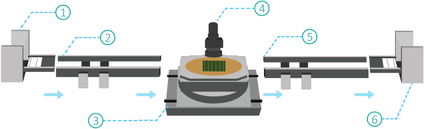
Modules
- Input
Wafer Magazine - XY Stage
- Wire Bond Vision Inspection
- Output
Wafer Magazine
Flowchart
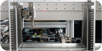
Transfer of wafer ring from the upstream machine or wafer magazine to the XY stage.
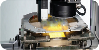
2D decoding and PR vision.
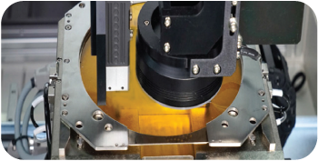
Wire bond vision inspection.
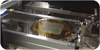
Transfer to the downstream machine or output after inspection is complete.
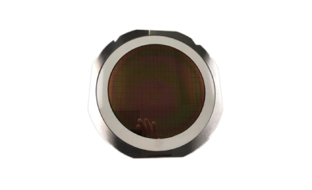
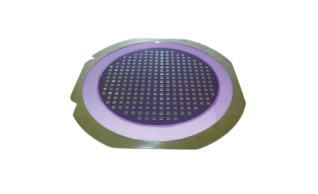
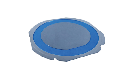
Wafer Ring (4 – 6 inches)
PCBA Tiles
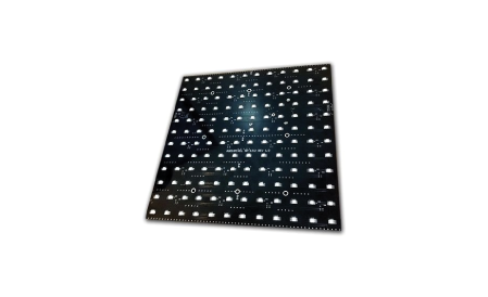
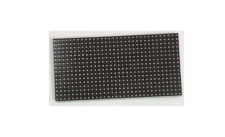
Top Inspection
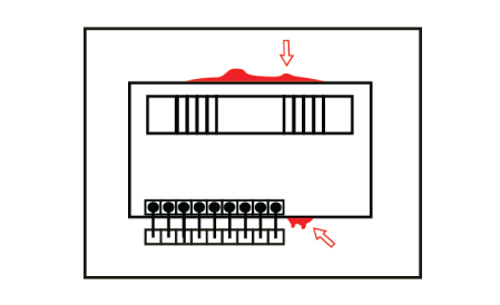
Glue Overflow in terms of Y
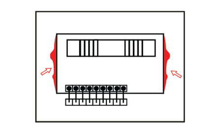
Glue Overflow in terms of X
Glue on Die
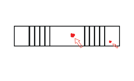
Die Missing
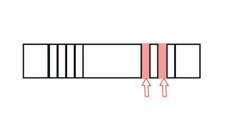
Die Chip
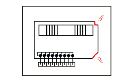
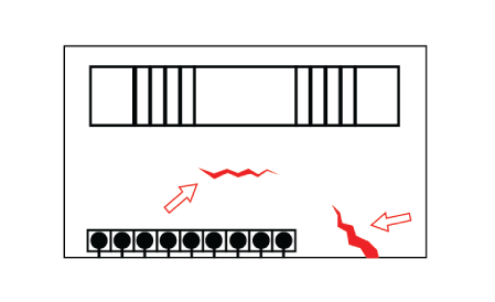
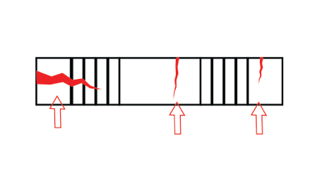
Die Crack
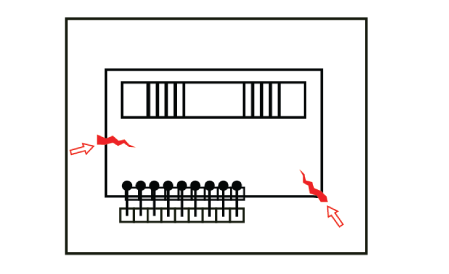
Die Scratches at Non-active Area
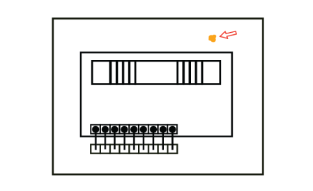
Die Scratches in PD Area
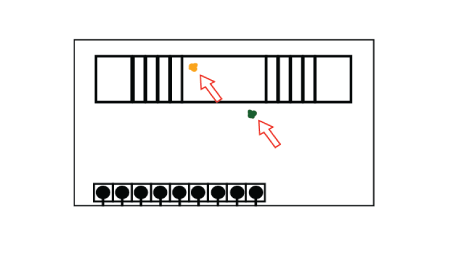
Foreign Material on PCB
Foreign Material on Die
Die Rotation
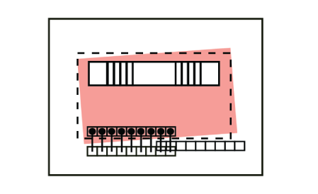
Die Misalignment
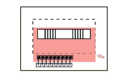
Wire Sweep
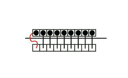
Missing Wire
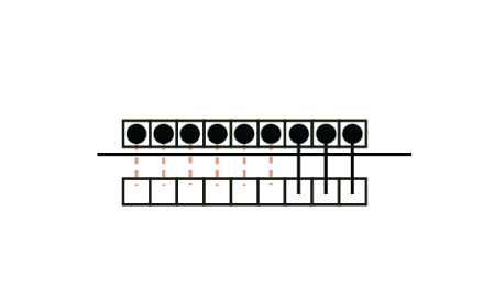
Non-stick on Pad (NSOP)
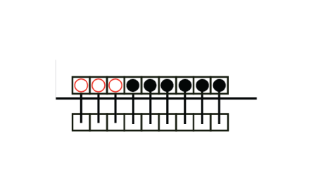
Non-stick on Lead (NSOL)
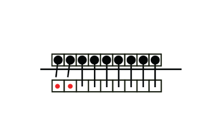
Unbonded
Smash Bond
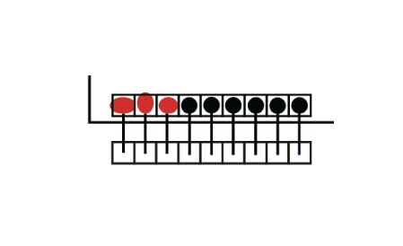
Bond Offset
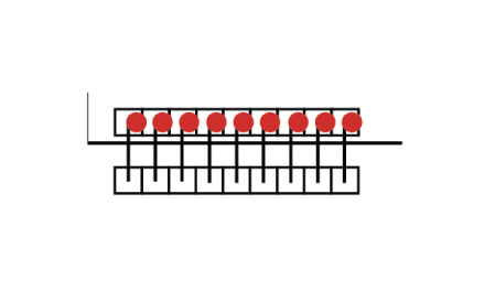
Double Bond
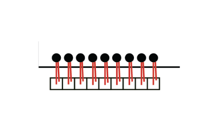
Bond Tail
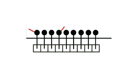
Broken Wire
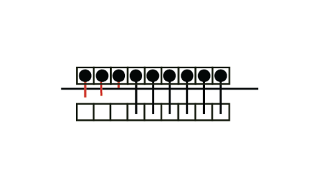
Vision Specifications
| Top Vision | ||
| Camera | 65MP Area Scan (Color) | |
| Accuracy | +/-3.5μm | |
| FOV (H x V) | 14.9mm x 11.2mm | |
| Magnification | 2x | |
| PR Vision | ||
| Camera | 1.3MP Area Scan (Mono) | |
| Accuracy | +/-0.25mm | |
| FOV (H x V) | 150mm x 110mm | |
Machine Specifications
| Products | 4” – 6” wafer | |
| Specifications | Input: | Tiles, Wafer, Wafer rings |
| Output: | Tiles, Wafer, Wafer rings | |
| UPH | 10K (single grab), 20K (multiple grab)
(depending on user product) |
|
| Vision Inspection | Wire Bond and Cosmetic | |
| Footprint | 1250mm (W) x 2400mm (L) x 2050mm (H) | |
| Warranty | 1 year limited excluding wear and tear parts | |
FAQ
What is a wire bond inspection machine?
A wire bond inspection machine is an automated optical inspection (AOI) system used to verify wire bond quality, bond placement accuracy, loop geometry, and packaging integrity in semiconductor manufacturing.
Why is automated wire bond inspection important?
Automated wire bond inspection eliminates human inspection variability, increases defect detection rates, improves production yield, and ensures compliance with automotive and semiconductor quality standards.
What types of wire bond defects can the Wi300 detect?
The WI300 detects a comprehensive range of wire bond defects, including lifted bonds, missing wires, wire sag, loop height deviations, bridging and misaligned bond pads, all at a minimum detectable size of 5um × 5um.
Is the WI300 compatible with existing wafer map systems?
Yes. The WI300 outputs STIF-format wafer map files, which are compatible with most semiconductor MES and ERP platforms. Custom format integration is available on request.
Can it handle warped or non-planar wafers?
Yes. The built-in confocal displacement sensor detects wafer warpage and automatically compensates height deviations up to 2mm without requiring manual fixture changes.
What wafer sizes does the WI300 support?
The WI300 supports wafers from 4″ tiles up to 12″ full wafers, covering a wide range of semiconductor front-end production formats.
What industries use the WI300?
The WI300 is deployed in semiconductor front-end assembly, LED/optoelectronics, power semiconductors, automotive electronics, and medical device manufacturing — any application requiring 100% inline wire bond quality assurance.
How does the WI300 compare to manual or sampling-based inspection?
Unlike manual inspection or sampling, the WI300 delivers 100% automated in-line coverage at production speed, eliminating human error, reducing inspection labour, and providing traceable digital quality records for every wafer.
Is the WI300 suitable for automotive EV electronic assembly lines?
Absolutely. EV power modules require heavy wiring that carries intense current under continuous vibration. The WI300 provides the high-resolution tracking needed to enforce zero-escape quality standards for critical automotive sensors, ECUs, and inverters.
How does the WI300 integrate with Smart Factory AI systems?
The machine features full SECS/GEM communication protocols. It instantly packages inspection tracking data and STIF wafer maps, allowing centralized factory AI algorithms to monitor microscopic process variations over time and optimize active wafer die and wire bond inspection system runs automatically.
What is wafer mapping in semiconductor inspection?
Wafer mapping is the process of visually displaying inspection results across a wafer, allowing engineers to identify defect patterns, monitor process stability, and improve manufacturing yield.
What are the vision inspection capabilities of MMS?
For a more detailed overview of our vision inspection capabilities, please visit https://mmsis.com/product-category/vision/ or send us an enquiry to discuss a solution tailored to your application requirements.
Does MMS offer other wafer inspection machines?
Yes, MMS offers a wide range of wafer inspection solutions for semiconductor manufacturing and quality assurance needs. View the full range at https://mmsis.com/product-category/front-of-line/ or contact us via the quick buttons on the side of the screen to reach us through your preferred channel.