Manual Table Input
Top Vision Inspection
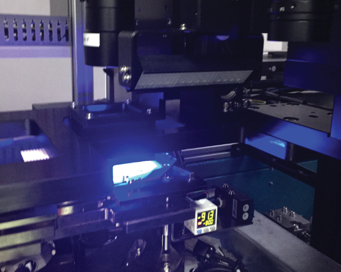
WI 400 Semi Auto Wafer Inspection is designed to deliver the utmost flexibility to support top vision inspection for fabricated components on wafer such as lens, LED & IC packages from 4” tiles to 8” wafer. With unique blend of flexibility and high performance, it makes an ideal inspection solution for automation industry.
Features
- Equipped with high-resolution camera
- Selection from 5MP to 25MP mono/colour camera imaging technology
- Integrated techniques
- Colour inspection, normalized correlation and rule-based algorithms
- Software alignment function
- Adjust wafer alignment angle for top vision inspection
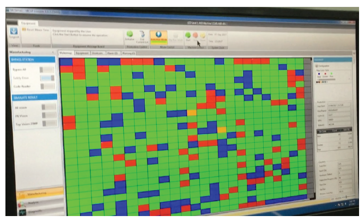
- Real time wafer map display
- All inspection information like mapping map, defect region, inspection result is visualized for easy reading
- Support common wafer map output format
- STIF files
- SPC statistical tool to monitor yield trend/ defect breakdown
- Minimum detectable defect size 15 μm x 15 μm
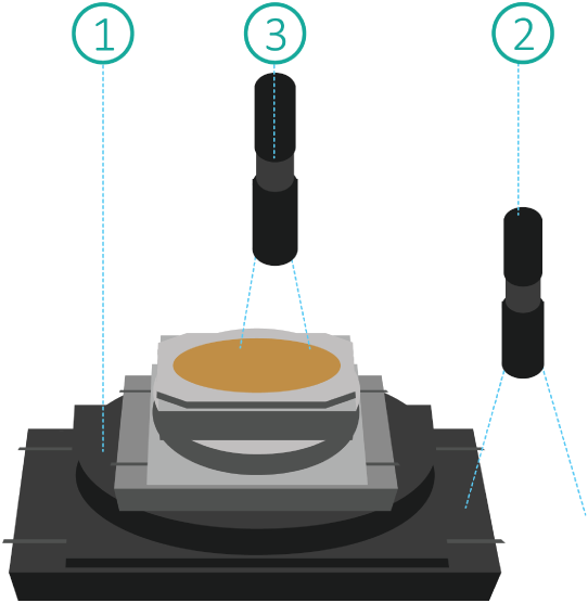
- Confocal displacement sensor for warpage detection. Height compensation up to 2mm
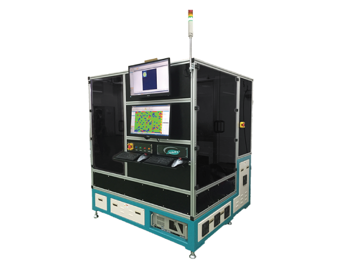
SEMI AUTO WAFER INSPECTION / WI400
Modules
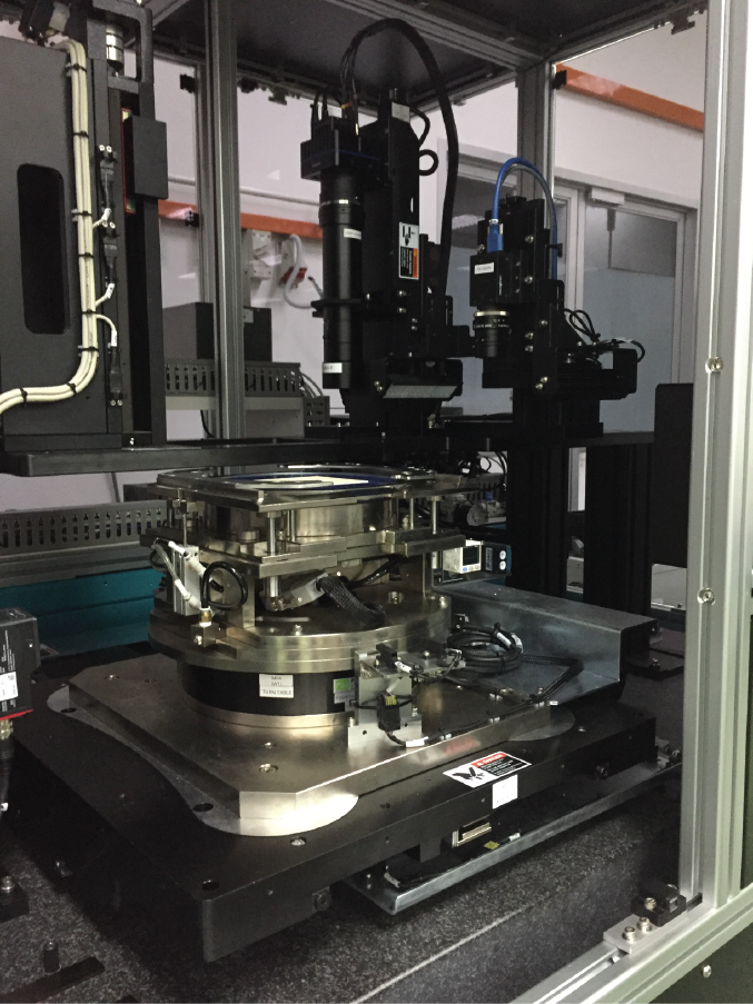
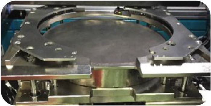
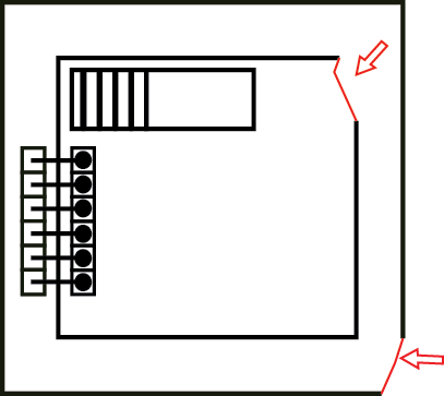
- Input
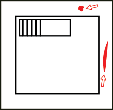
XY Table - OCR Vision
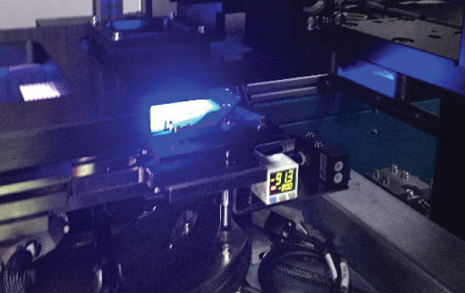
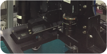
To capture entire wafer product code for e-map processing - Top Vision Inspection Module
Flowchart
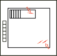
- The product is manually placed on top of the XY table. The table then carries the product to the OCR vision test site.
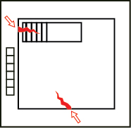
OCR vision reads the code on the wafer in order to record the result for the wafer to be loaded, preventing the result from being lost.
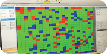
XY offset is corrected before top vision inspection. Real-time wafer mapping results are displayed as the inspection is running.
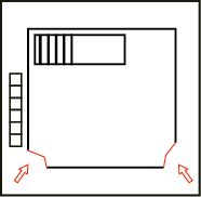
Once complete, the table moves back to the load/unload position, and the product can be safely unloaded.
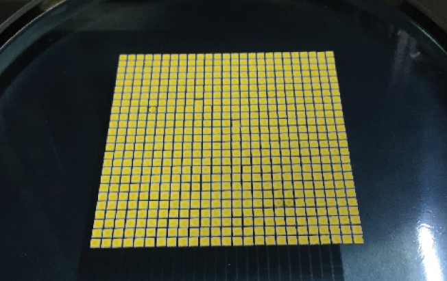
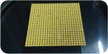
Bare Wafer
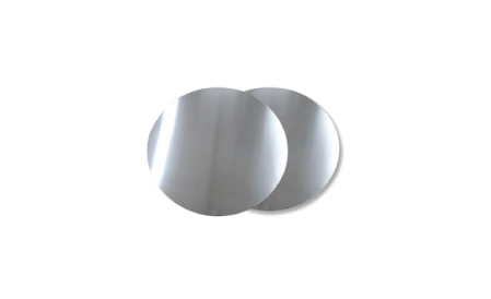
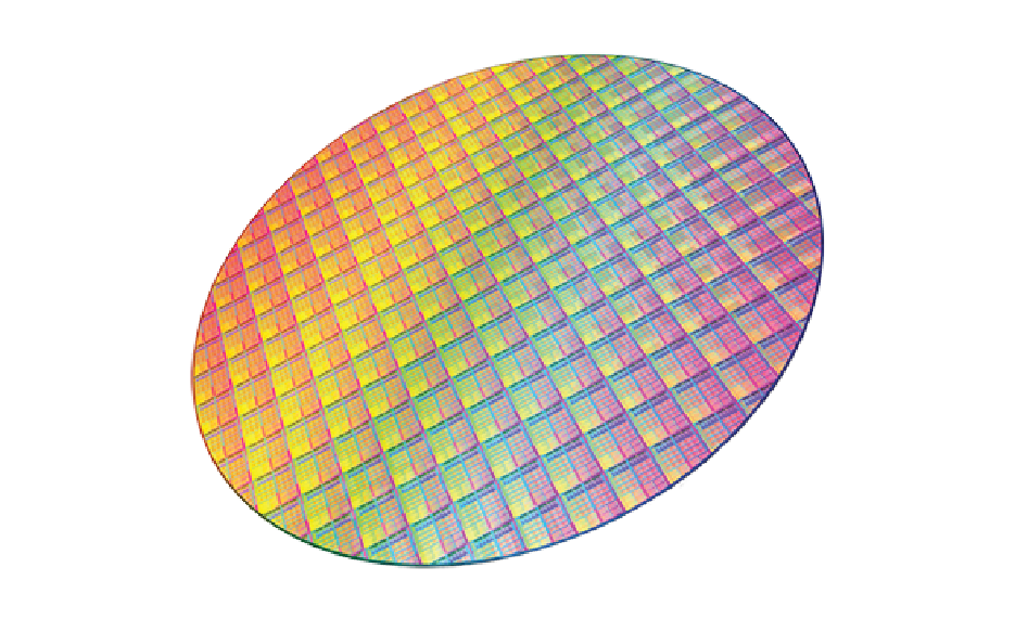
Wafer
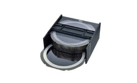
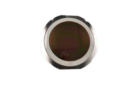
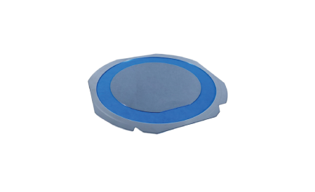
Wafer Ring
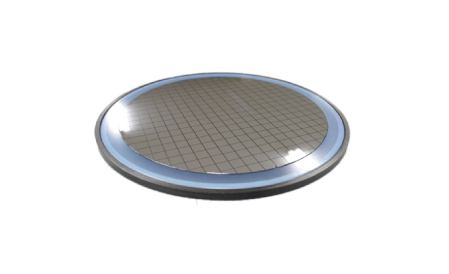
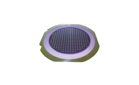
Top Inspection
Foreign Material
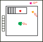
Stains
Scratches
Chipping
Cracked
Damaged Bump
Discoloration
Lifted Metal
Measuring
Un-separation
| Products | 6” bare wafer or 8” wafer ring | |
| Specifications | Input: | Bare wafer, Wafer rings |
| Output: | Tiles, Wafer, Wafer rings | |
| UPH | 10K (depending on user product) | |
| Vision Inspection | Cosmetic | |
| Footprint | 1250mm(W) x 1600mm(L) x 2100mm(H) | |
| Warranty | 1 year limited excluding wear and tear parts | |
Wafer Inspection Machine for Perfect Bare Wafer Analysis
In today’s semiconductor industry, accuracy is everything. A wafer inspection machine plays a pivotal role in ensuring each wafer meets the strictest quality standards before fabrication begins. Our state-of-the-art inspection systems are engineered with precision optics and intelligent automation to detect even the most microscopic surface defects and particles across bare wafers, guaranteeing exceptional yield and performance consistency.
Designed for research labs and high-volume production lines alike, this advanced bare wafer inspection technology integrates automated handling, high-resolution imaging, and AI-driven classification. It allows semiconductor engineers to visualise, quantify, and analyse defects faster and with greater confidence — reducing downtime and enhancing overall manufacturing reliability.
Backed by years of engineering expertise and continuous innovation, our inspection solutions align with global SEMI standards and support a wide range of wafer sizes. Each unit undergoes rigorous testing to ensure stability, repeatability, and long-term precision.
Empower your production line with technology built on trust, accuracy, and expertise. Discover how our wafer inspection machines can elevate your semiconductor quality — contact our team today for a personalised consultation.