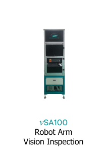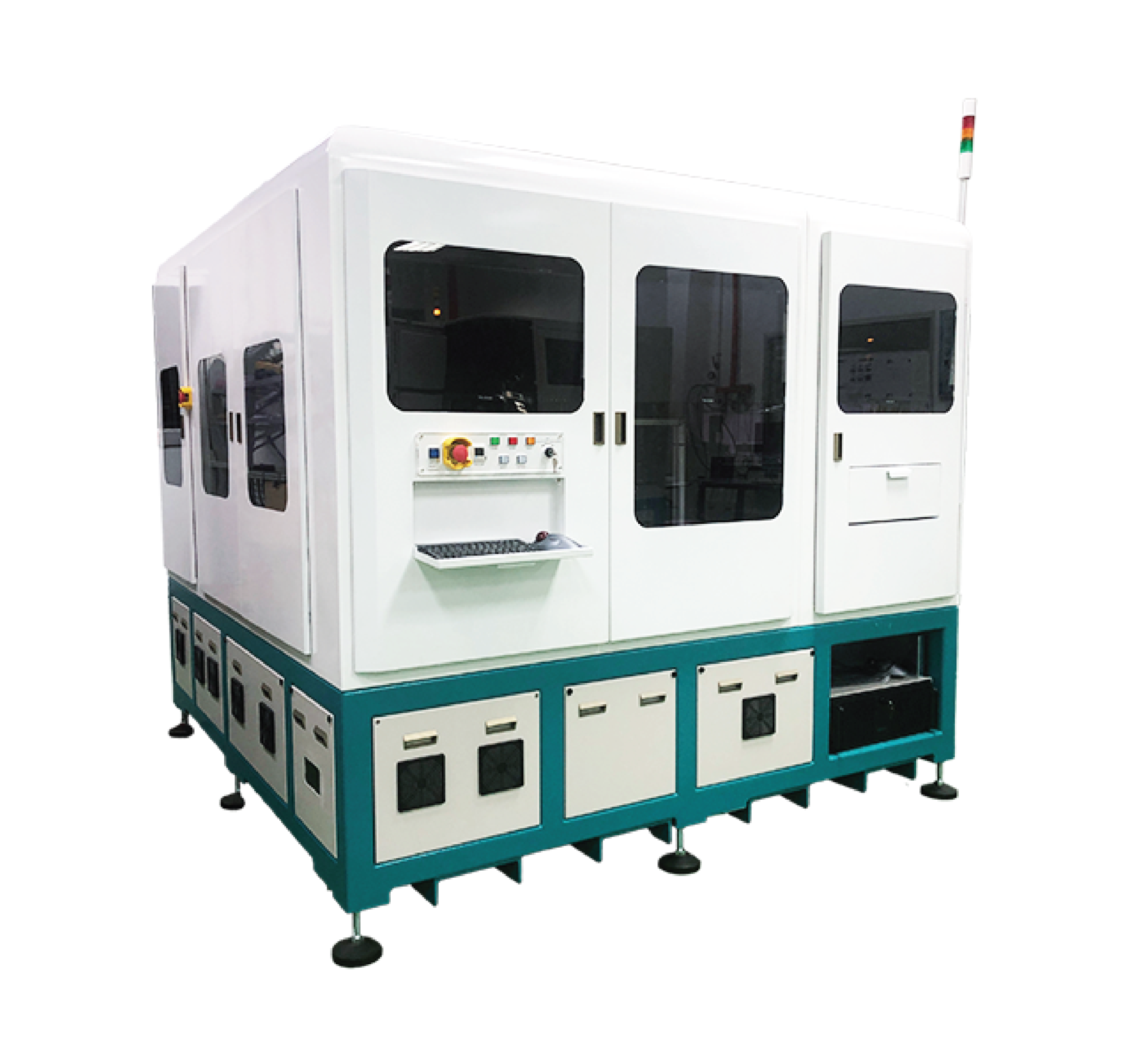
Modules
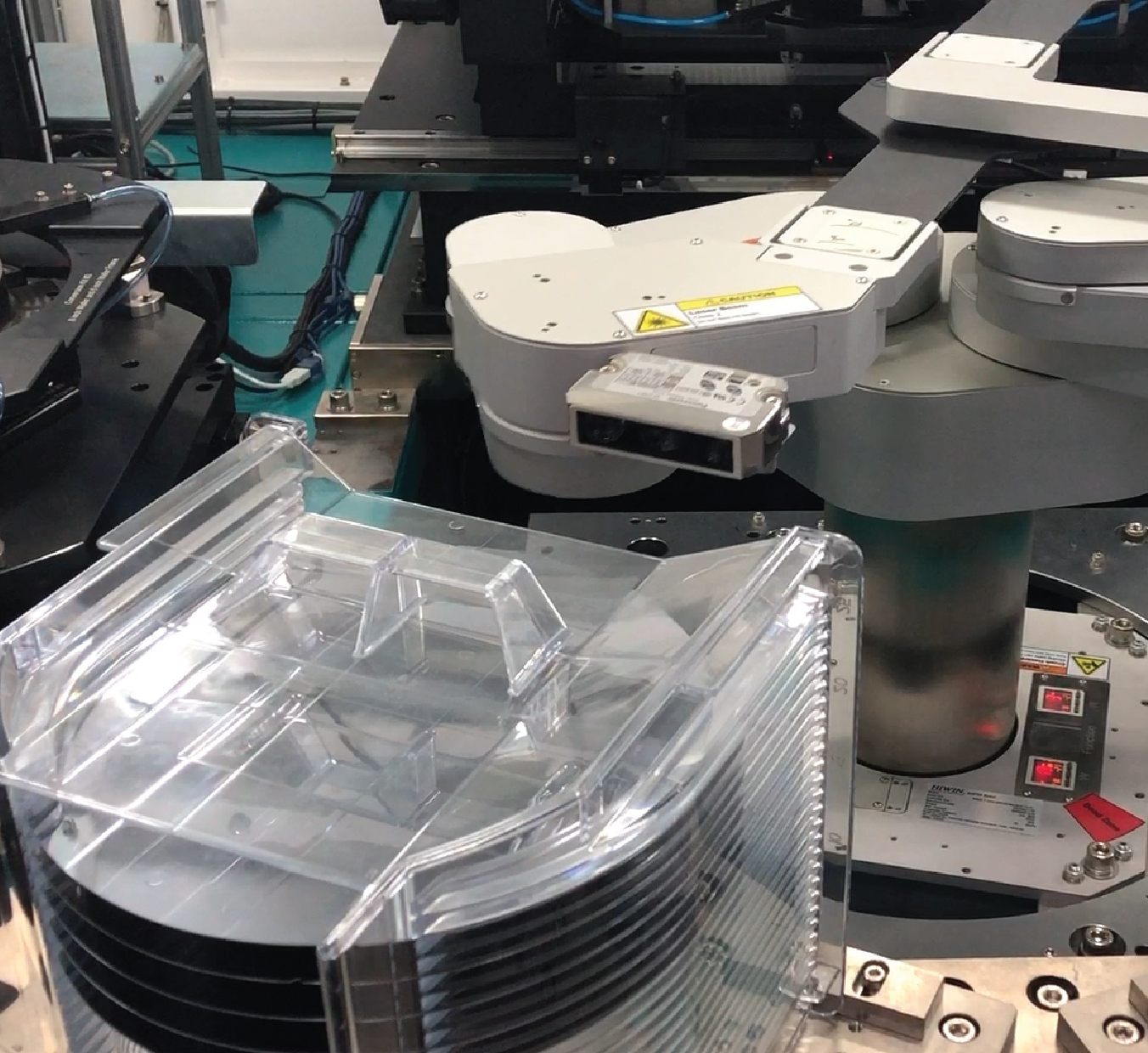
- Input/Output Wafer Cassette Station
- Dual-Arm Wafer Robot
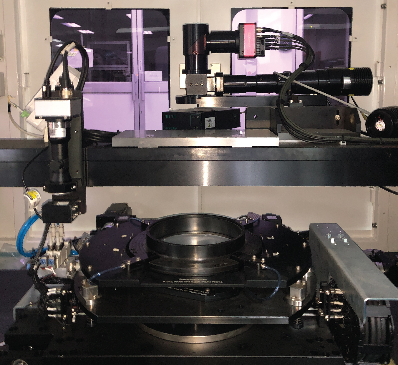
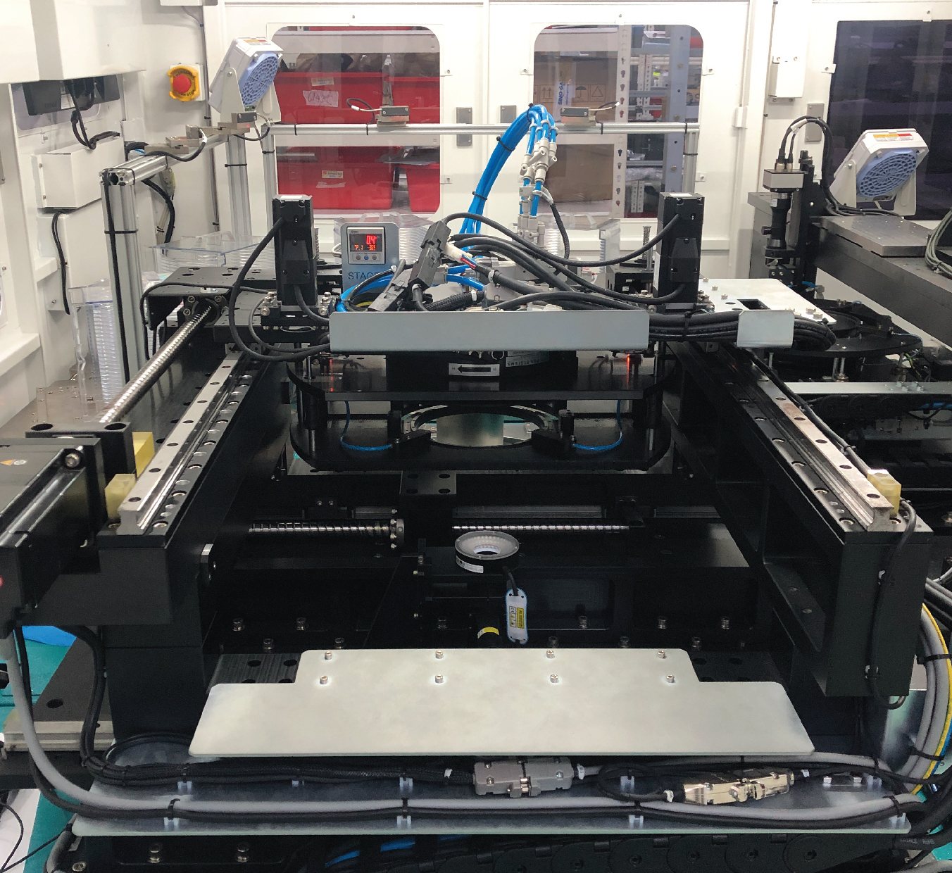
- XYZθ Stage
- Aligner Vision Inspection
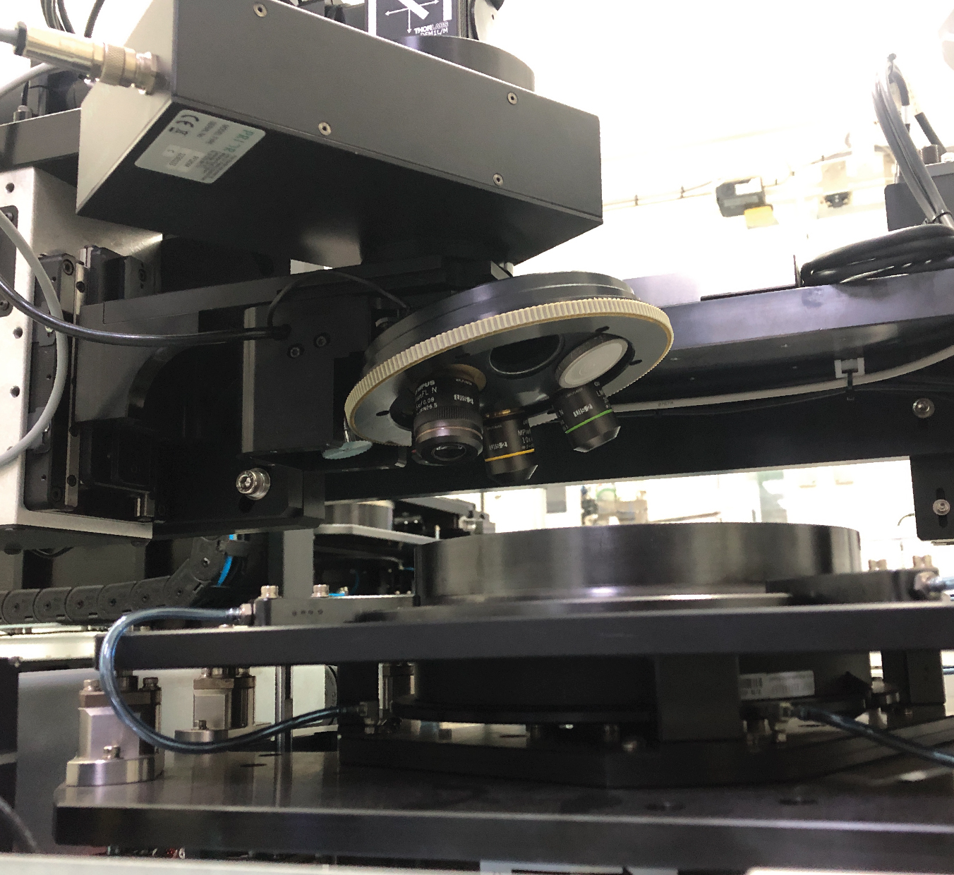
- Auto Focus Top Vision Inspection
- Bottom Vision Inspection
Flowchart
Wafer robot carries wafer onto xyzθ stage to perform aligner vision inspection after its mapping sensor determines the status of wafer insertion in the input cassette.
The xyzθ stage transfers wafer under top vision for defects inspection after align position and orientation of wafer.
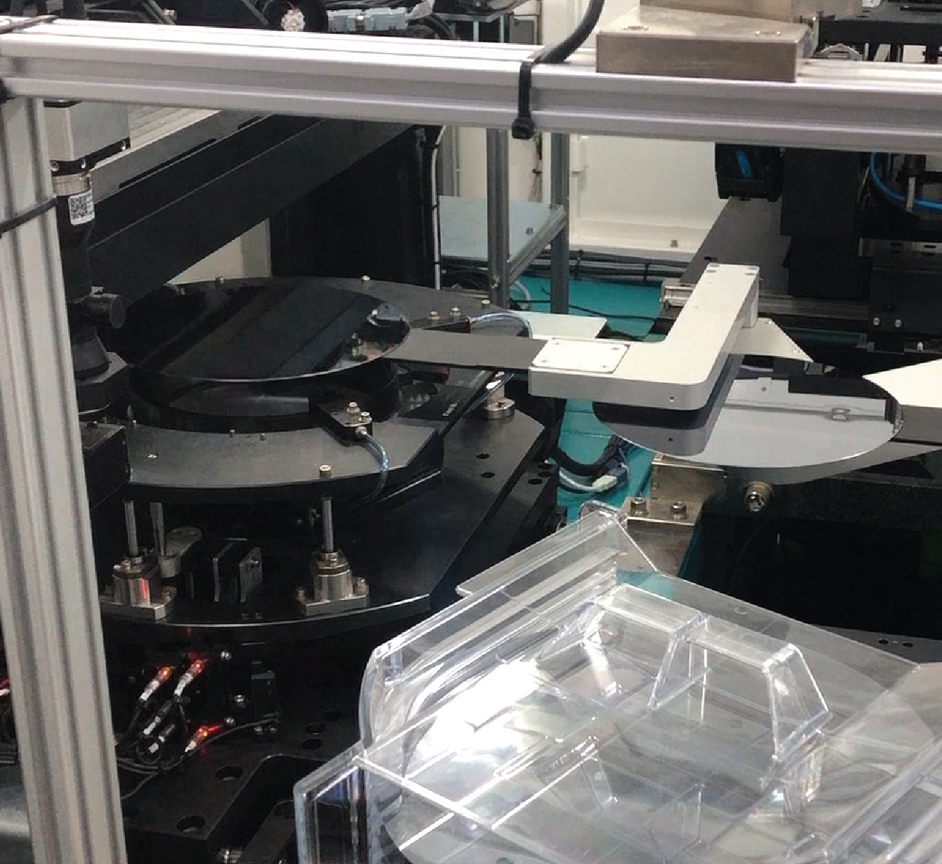
Right robot arm transfers inspected wafer to bottom vision’s stage while left robot arm simultaneously loads next wafer to vision aligner’s stage.
The xyzθ stage transfers inspected wafer under bottom vision for defects inspection.
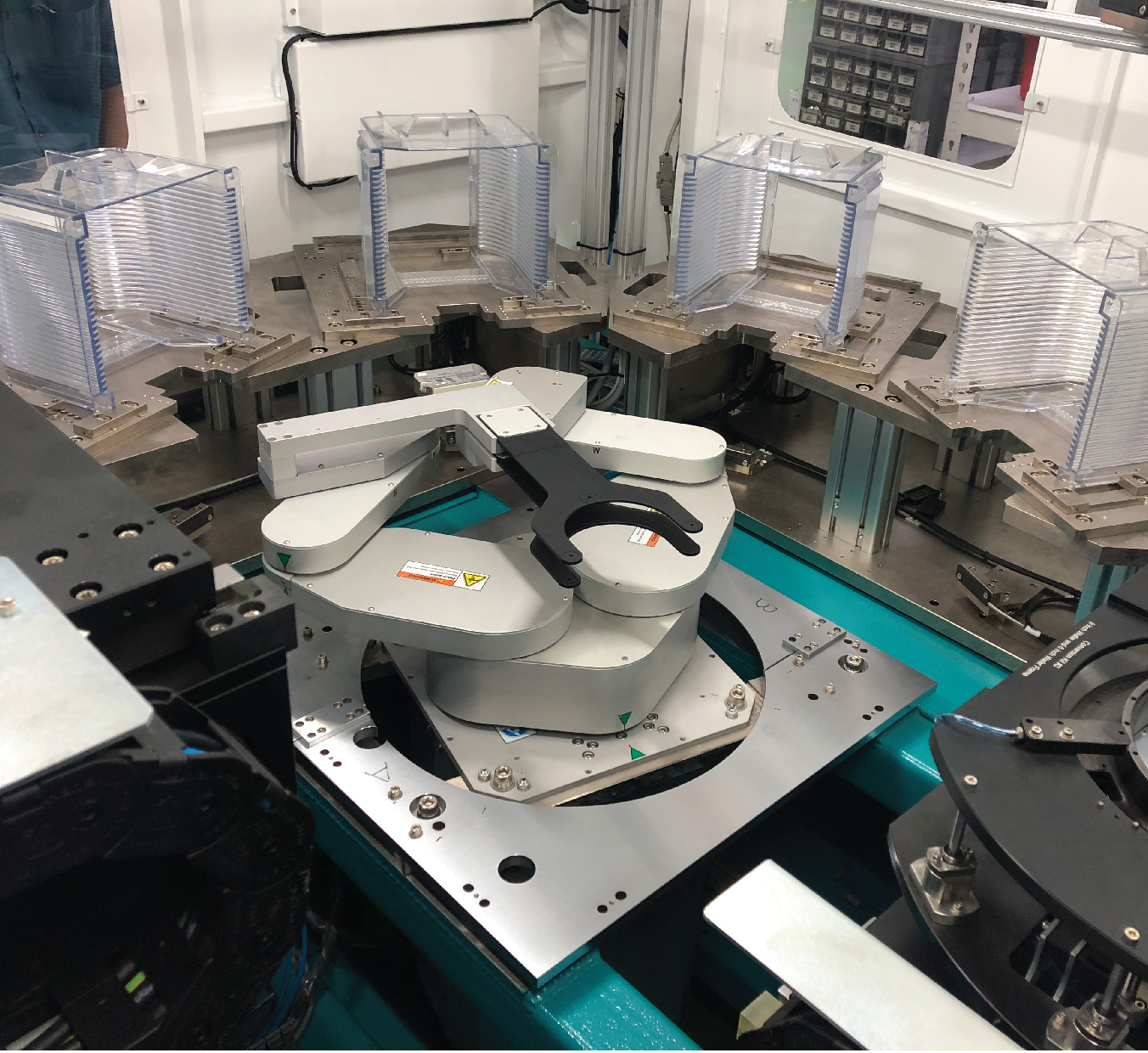
Wafer robot unload fully inspected wafer into output cassette.
Inspection result will be display on monitor during top and bottom inspection process.
Features
- Versatile Product Support Compatibility
- Supports 4” to 12” wafer and 4” to 8” wafer frame
- Die/Chip size: 76–1770μm, Die thickness: 75–750μm
- Customizable Top & Bottom Vision Inspection
- Multiple camera selection options to match die sizes for precise inspection
- High-precision 4 objective lens turret for superior accuracy and flexible FOV
- Advanced Vision Aligner System
- Detects and corrects wafer position and angle for optimal alignment
- Configurable xyzθ Stage
- Convertible minimum-contact vacuum chuck for sensitive wafer handling
- Bottom vision inspection capability on the xyzθ stage
- Attachable glass option for inspecting sensitive thin wafers
- Support various end effector forks
- 360° rotary for vision aligner
- Dual-Arm Wafer Robot
- Wide range of optional end effector & mapping sensor is available
- Flexible Input/Output Cassette System
- Up to 4 cassettes for 6” & 8” wafers/wafer frames
- Up to 2 cassettes for 12” wafers
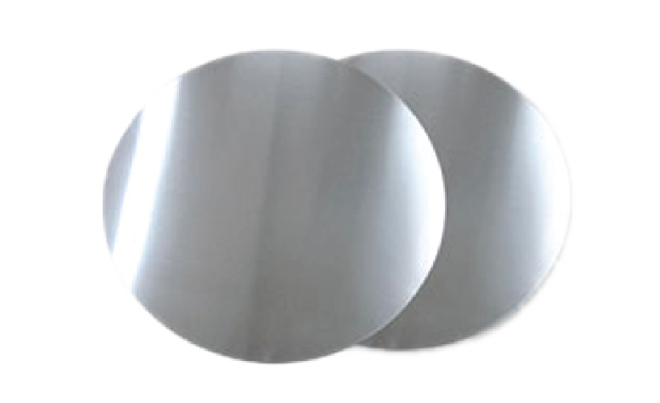
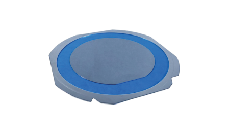
Bare Wafer / Wafer / Wafer Frame
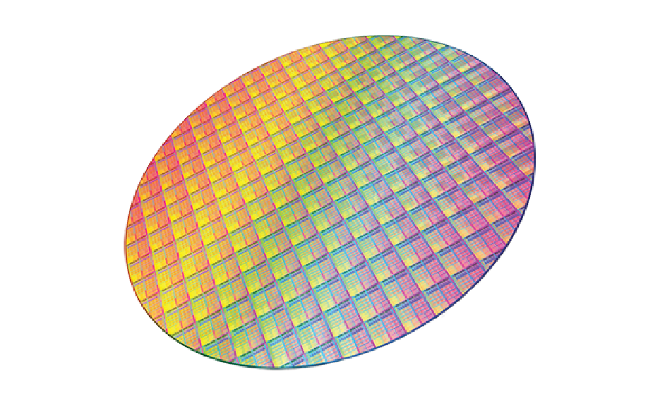
Top Vision Inspection
Wafer Defects
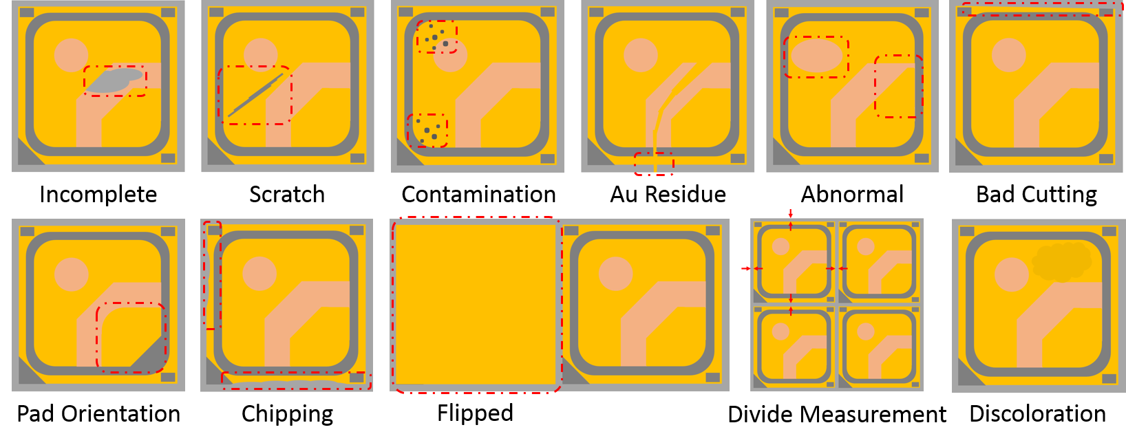
Wafer Frame Defects
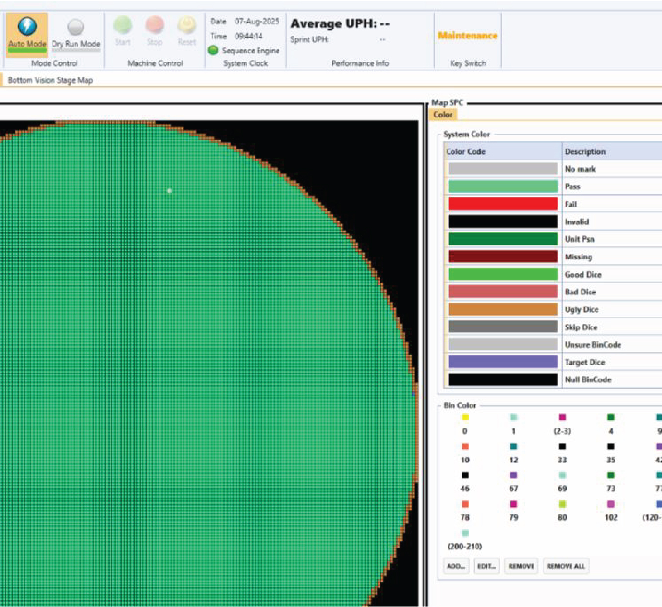
Bottom Vision Inspection
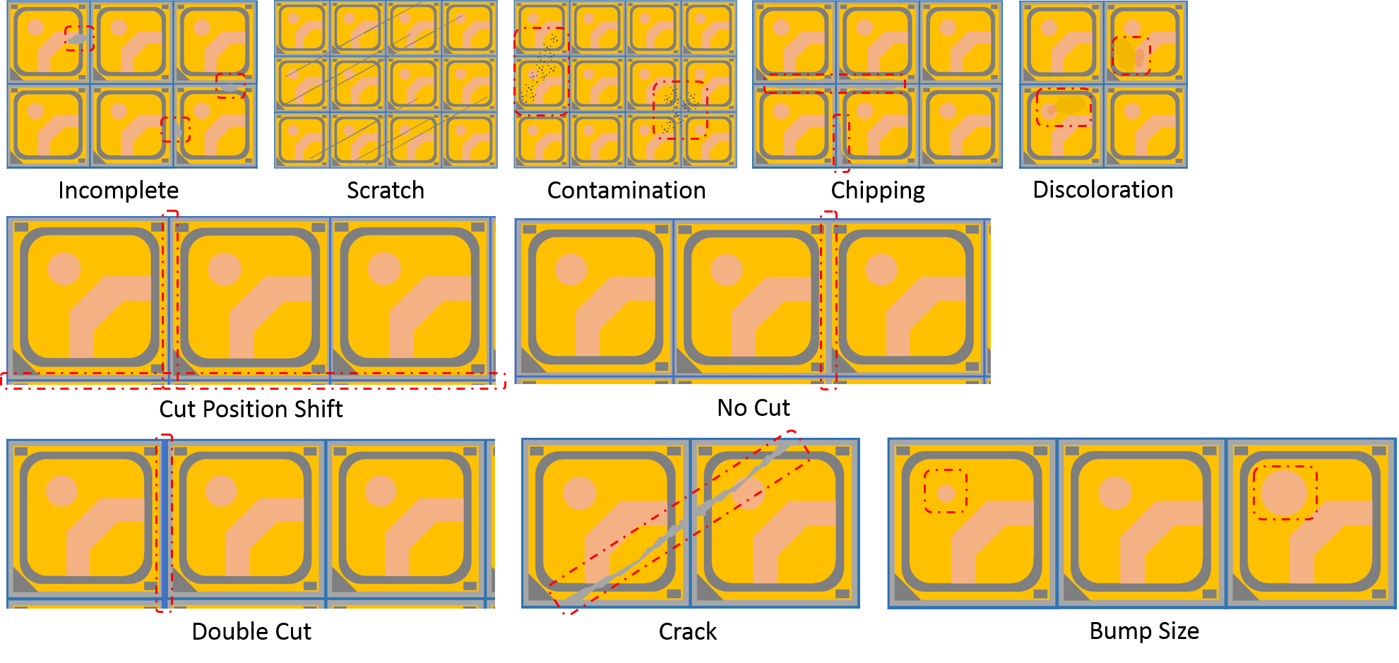
Wafer Defects
Wafer Frame Defects
Vision Specifications
| Aligner Vision | |||||
| Camera | 2K Line Scan Mono | ||||
| FOV (H x V) | ~17mm (H) | ||||
| Magnification | 1X Telecentric Lens | ||||
| Accuracy | ±20μm | ||||
| Min. Detectability | ~40μm | ||||
| Inspection Criteria | Inspection orientation in xy0 (Flat and Notch) | ||||
| Top Vision | |||||
| Camera | 25MP Area Scan Color | ||||
| FOV (H x V) | 0.65~5.1mm x 0.64~5.1mm | ||||
| Magnification | Lens Turret with 4 Objective Lens: 2.5X, 5X, 10X, 20X (Customisable) | ||||
| Accuracy | ±10μm, ±5μm, ±2.5μm, ±2μm | ||||
| Min. Detectability | ~20μm, ~10μm, ~5μm, ~4μm | ||||
| Inspection Criteria | Wafer (No Dicing) a. Scratch/Crack b. Discolouration c. Wafer Broken d. Contamination/Dirt Wafer Frame (Dicing – Singulated) a. Chipping b. Scratch/Crack c. Discolouration d. Cut Inspection (No Cut/Half-Cut/Cut Position) e. Bump Size (Diameter) f. Contamination/Dirt |
||||
| Bottom Vision | |||||
| Camera | 25MP Area Scan Color | ||||
| FOV (H x V) | 6.4mm x 6.4mm | ||||
| Magnification | 2X Telecentric Lens | ||||
| Accuracy | ±5μm | ||||
| Min. Detectability | ~10μm | ||||
| Inspection Criteria | Wafer (No Dicing) a. Scratch/Crack b. Discolouration c. Wafer Broken d. Contamination/Dirt Wafer Frame (Dicing – Singulated) a. Scratch/Crack b. Wafer Broken c. Contamination/Dirt |
||||
Machine Specifications
| Products | Wafer | 4” to 12” wafer | |||
| Wafer Frame | 4” to 8” wafer frame | ||||
| Die Chip | Size: 76~1770μm | ||||
| Thickness: 75~750μm | |||||
| Wafer Robot | Arms Quantity | Dual Arm ( Optional: Single Arm only) | |||
| Ends Effector | Non-contact Bernoulli / Non-contact Edge Grip/ Vacuum / Passive-edge Holding / Porous / Gripper | ||||
| Input Output | Cassette Size & Quality |
4”, 6”, 8” Wafer/Wafer Frame: 2~4 Input Output Cassette | |||
| 12” Wafer: 1~2 Input Output Cassette | |||||
| Top & Bottom Vision Inspection | Objective Lens / Telecentric Lens | ||||
| xyθ Stage | Vacuum Chuck (Top & Bottom Vision Inspection) |
||||
| Kit 1: 4” Wafer | |||||
| Kit 2: 6” Wafer & 4” Wafer Frame | |||||
| Kit 3: 8” Wafer & 6” Wafer Frame | |||||
| Kit 4: 12” Wafer & 8” Wafer Frame | |||||
| Rated Wafer Per Hour | 4”: 70 WPH | 6”: 30 WPH | 8”: 15 WPH | 12”: 6 WPH | |
| Footprint | 2200mm (W) x 2200mm (L) x 2000mm (H) | ||||
| Warranty | 1 year limited excluding wear and tear parts | ||||
Auto Focus Wafer Inspection Machine for Reliable Bare Wafer Inspection
In semiconductor manufacturing, small defects on bare wafers or frames can quickly turn into yield loss, rework, and unplanned downtime. An auto focus wafer inspection machine ensures consistent, repeatable bare wafer inspection by automatically optimising focus and image quality for each die and frame area. This helps process and QA teams maintain stable quality standards, especially in high-mix, high-volume environments.
The system is designed to tackle the real-world quality issues that often slip through traditional inspection:
- Wafer defects (top and bottom vision)
incomplete die, scratches, contamination, Au residue, and other surface irregularities.
- Wafer frame defects (top vision)
incomplete cuts, cut position shift, double cuts, scratches, no cut, contamination, cracks.
- Wafer frame defects (bottom vision)
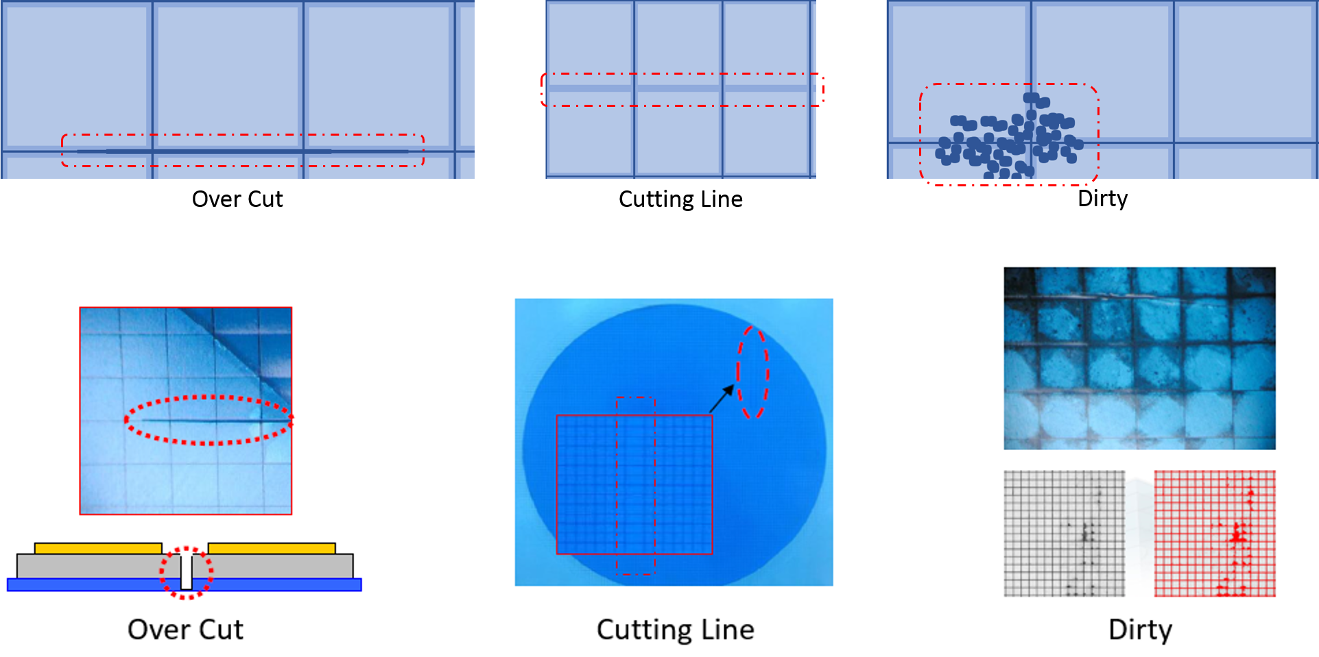
over cuts, cutting line issues, dirty or contaminated frame areas.
By consolidating these inspections into one automated wafer inspection machine, manufacturers can reduce escapes, improve first-pass yield, and react faster to process drift.
Why Choose This Auto Focus Wafer Inspection Machine
This platform stands out by combining customisable, AI-ready vision inspection with intelligent material handling. Moreover, multiple camera options allow the vision system to be matched to different die sizes and thicknesses, while inspection settings can be fine-tuned for each product. Its architecture is designed for AI integration, enabling advanced defect detection, classification, and trend analysis to enhance the consistency of bare wafer inspection over time.
At the same time, a configurable xyzθ stage with a minimum-contact vacuum chuck positions wafers at the ideal angle and height, supports thin and sensitive wafers, and allows bottom vision inspection directly on the stage for better repeatability. This is complemented by a dual robot arm configuration with flexible end effector and mapping options, as well as multiple input/output cassette configurations for various wafer and frame sizes. Together, these features make this auto focus wafer inspection machine a robust and scalable choice for fabs and OSATs that need stable, high-quality bare wafer inspection.