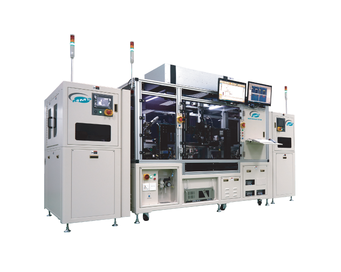
Wafer Wire Bond Inspection Machine | WI300
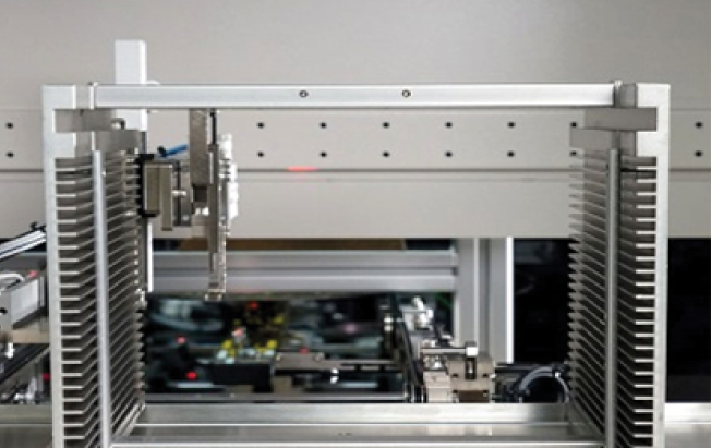
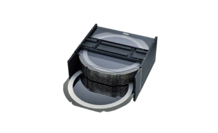
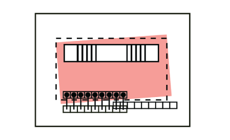
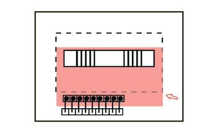
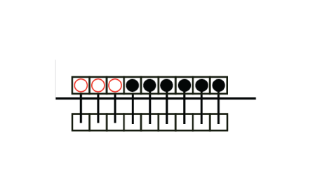
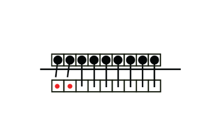
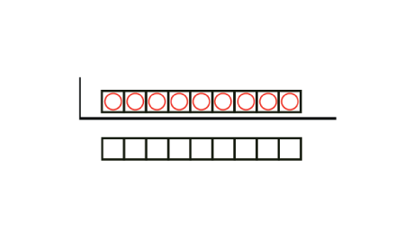
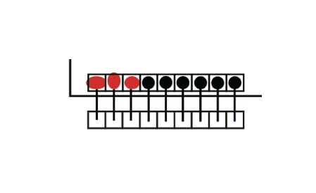
Wafer Magazine
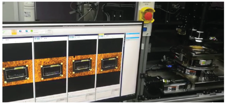
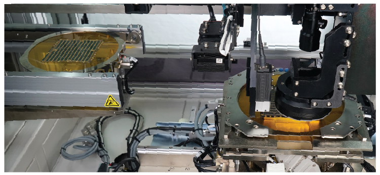
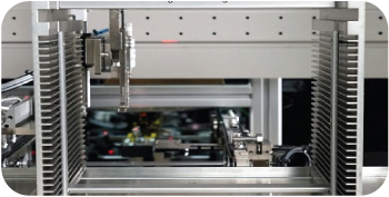
Top Vision Inspection
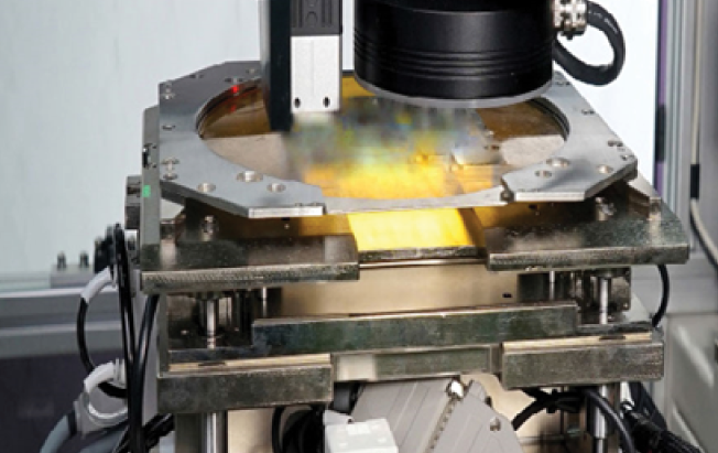
WI 300 Wafer Inspection Machine is designed to deliver utmost flexibility to support top vision inspection for fabricated components on wafer such as lens, LED & IC packages from 4” tiles to 6” wafer. With unique blend of flexibility and high performance, it makes an ideal inspection solution for automation industry.
Features
- High-Resolution Camera
- Selection from 5MP to 65MP mono/colour camera imaging technology
- Wafer Die and Wire Bond Inspection
- Cosmetic and Wire Bond Checking
- Auto Alignment Function
- 2D decoding and Position Recognize (PR) vision
- Real-Time Wafer Map Display
- All inspection information, such as mapping maps and defect region inspection results, is visualized for easy reading
- Supports Common Wafer Map Output Formats
- STIF Files
- Minimum Defect Size
- 5μm x 5μm
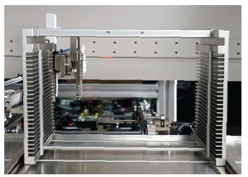
- Confocal Displacement Sensor
- For warpage detection and height compensation up to 2mm
-
Multiple Unit Inspection in a Single Grab
Fully Auto Wafer Inspection / WI300
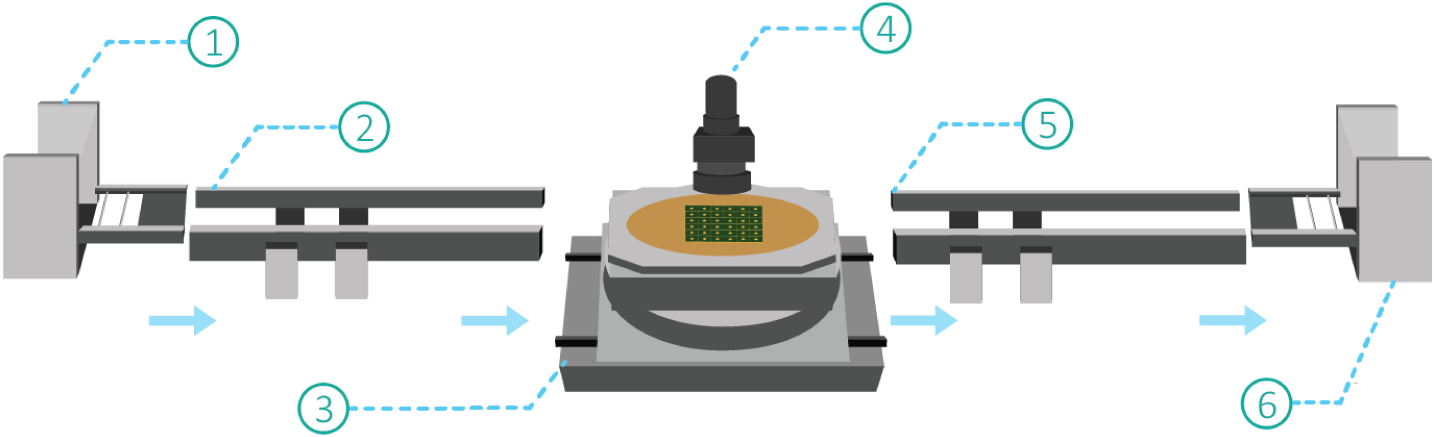
Modules
- Input
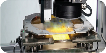
Wafer Magazine - XY Stage
- Wire Bond Vision Inspection
- Output
Wafer Magazine
Flowchart
Transfer of wafer ring from the upstream machine or wafer magazine to the XY stage.
2D decoding and PR vision.
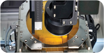
Wire bond vision inspection.
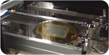
Transfer to the downstream machine or output after inspection is complete.
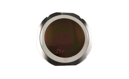
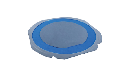
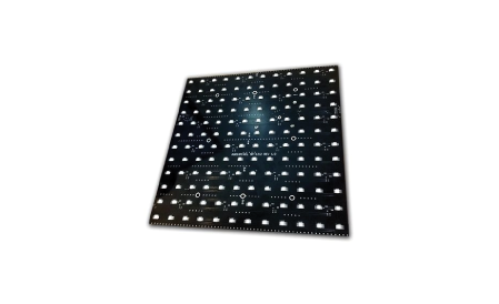
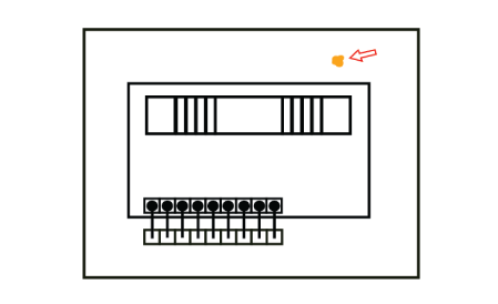
Wafer Ring (4 – 6 inches)
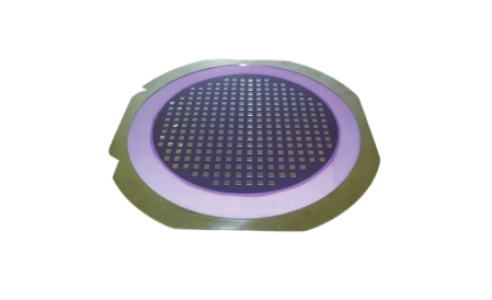
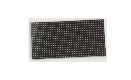
PCBA Tiles
Top Inspection
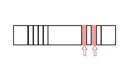
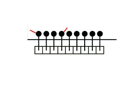
Glue Overflow in terms of Y
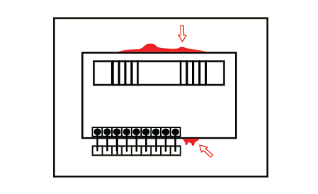
Glue Overflow in terms of X
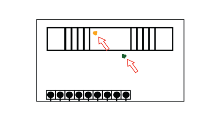
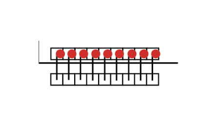
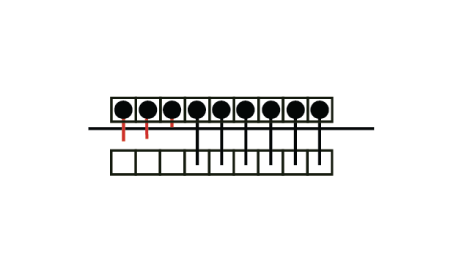
Glue on Die
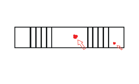
Die Missing
Die Chip
Die Crack
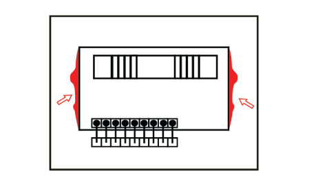
Die Scratches at Non-active Area
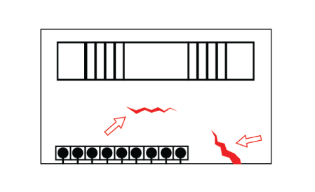
Die Scratches in PD Area
Foreign Material on PCB
Foreign Material on Die
Die Rotation
Die Misalignment
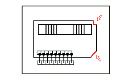
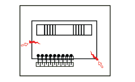
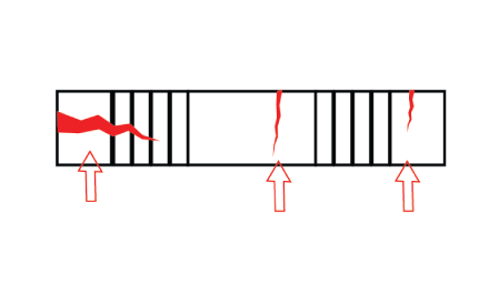
Wire Sweep
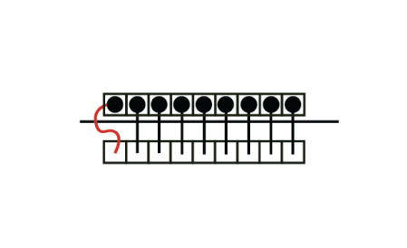
Missing Wire
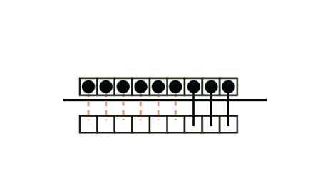
Non-stick on Pad (NSOP)
Non-stick on Lead (NSOL)
Unbonded
Smash Bond
Bond Offset
Double Bond
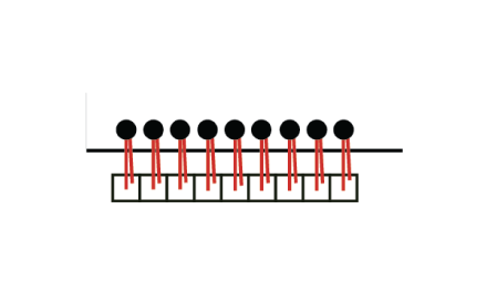
Bond Tail
Broken Wire
Vision Specifications
| Top Vision | ||
| Camera | 65MP Area Scan (Color) | |
| Accuracy | +/-3.5μm | |
| FOV (H x V) | 14.9mm x 11.2mm | |
| Magnification | 2x | |
| PR Vision | ||
| Camera | 1.3MP Area Scan (Mono) | |
| Accuracy | +/-0.25mm | |
| FOV (H x V) | 150mm x 110mm | |
Machine Specifications
| Products | 4” – 6” wafer | |
| Specifications | Input: | Tiles, Wafer, Wafer rings |
| Output: | Tiles, Wafer, Wafer rings | |
| UPH | 10K (single grab), 20K (multiple grab)
(depending on user product) |
|
| Vision Inspection | Wire Bond and Cosmetic | |
| Footprint | 1250mm (W) x 2400mm (L) x 2050mm (H) | |
| Warranty | 1 year limited excluding wear and tear parts | |