
Wire Bond Inspection: A Vital Process in Electronics Assembly
In the heart of semiconductor manufacturing, precision defines success. Every tiny connection matters — especially those invisible bonds linking silicon chips to their package leads. At this microscopic level, even the slightest deviation can jeopardize the performance of an entire electronic system. That’s why wire bond inspection has become an indispensable step in today’s advanced electronics assembly process.
Why is Wire Bond Integrity Important?
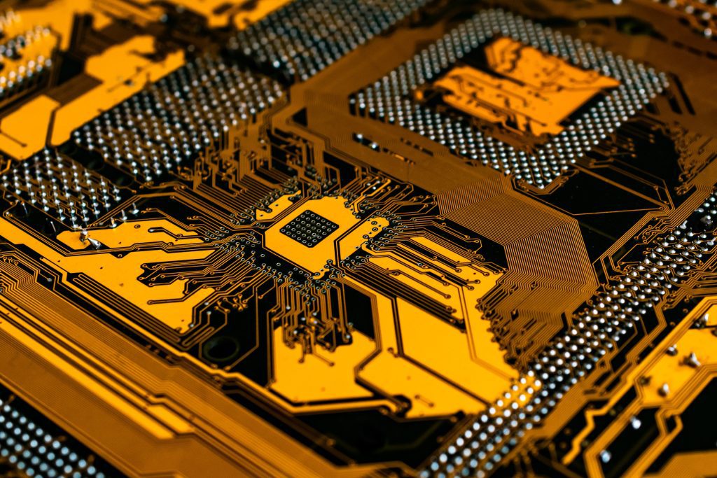
Wire bonding is the process of connecting a semiconductor die to its external circuitry using ultra-fine gold, aluminum, or copper wires. These connections serve as the nervous system of an integrated circuit, transmitting electrical signals with extreme precision. However, variations in bond strength, contamination, or alignment can compromise device reliability.
Through wire bond inspection, we ensure each interconnect meets stringent mechanical and electrical standards before the device moves forward in the production line. This process isn’t just about defect detection — it’s a critical safeguard that supports long-term reliability and product consistency across large-scale manufacturing.
Inspection Techniques In Modern Electronics Assembly
As Malaysia strengthens its role as a key player in global semiconductor assembly and test services, inspection technologies have evolved to match international expectations. Our industry employs multiple methods of wire bond inspection, each serving a distinct purpose in maintaining high yield and reliability:
- Optical and Laser Inspection: Automated optical inspection (AOI) systems use high-resolution cameras and laser triangulation to detect visible defects such as wire sweep, sagging, and misalignment. These non-contact systems provide real-time analysis during high-volume production.
- X-ray Inspection: This technique penetrates the encapsulant to reveal internal bond structures. It’s particularly valuable for verifying stitch bonds or detecting broken wires in hidden areas where visual inspection cannot reach.
- Pull and Shear Testing: Mechanical stress tests are performed to measure the bond’s strength at both the heel and ball joints. These tests confirm whether the wire can withstand thermal cycling and vibration stresses in the field.
- Acoustic Microscopy (C-SAM): High-frequency sound waves reveal delaminations, voids, and cracks around bonding interfaces. This non-destructive method helps identify potential failure zones before encapsulation.
By combining these techniques, we achieve a comprehensive evaluation of bond integrity — from structural analysis to performance prediction.
Common Defects Detected Through Inspection
The types of failures found through wire bond inspection vary based on materials and process conditions. Typical defects include non-stick on pad (NSOP), heel cracks, wire breaks, contamination, lifted bonds, and bond voids. Each of these faults can alter current flow or thermal dissipation, ultimately leading to electrical instability or total device failure.
Identifying these issues early prevents costly downstream rework and ensures that subsequent assembly stages — such as molding, encapsulation, and final testing — begin with a flawless foundation.
Data-Driven Quality Control In Semiconductor Manufacturing
In a data-centric industry, inspection systems no longer serve only as defect detectors. Today, they’re integrated into smart manufacturing ecosystems, providing actionable data that supports real-time process optimization. By analyzing bond strength distributions, thermal profiles, and image-based defect trends, we can fine-tune bonding parameters like ultrasonic power, bonding force, and time.
Such continuous monitoring transforms wire bond inspection from a traditional quality gate into a predictive tool for yield enhancement. In Malaysia’s growing semiconductor ecosystem — especially within Penang and Kulim’s advanced packaging clusters — these data insights are driving new standards in process control and traceability.
The Role Of Automation And Artificial Intelligence
Modern inspection platforms increasingly leverage artificial intelligence (AI) and machine learning algorithms to classify defects, minimize false calls, and accelerate decision-making. These systems learn from historical inspection data, enabling automatic differentiation between true process issues and benign variations.
By integrating AI with robotic handling, we enhance consistency and reduce operator dependency — key advantages for achieving zero-defect manufacturing targets demanded by global clients.
Ensuring Reliability From Bond To Board
Ultimately, wire bond inspection ensures that every connection between die and lead frame performs reliably throughout a product’s lifecycle. Whether it’s a microcontroller inside an automotive module or a high-frequency chip for 5G communication, dependable wire bonds are the foundation of electronic functionality.
As we continue advancing Malaysia’s position in high-value semiconductor assembly, our commitment to precise inspection and data-driven quality control remains essential. By combining innovative inspection techniques, AI-assisted analytics, and continuous improvement, we strengthen the reliability chain from bond to board — ensuring that every device leaving our production line meets the world’s highest expectations.