
Why Bare Wafer Inspection Is Vital for Semiconductor Manufacturing
The semiconductor industry thrives on precision. Every chip that powers our modern world—whether in smartphones, data centers, or electric vehicles—depends on materials engineered at atomic scales. At the foundation of this process lies the silicon wafer. Before any layer of circuitry is patterned, that wafer must be flawless. This is where bare wafer inspection becomes indispensable.
The Foundation Of Semiconductor Quality
In semiconductor fabrication, a single microscopic defect can derail millions of transistors. Bare wafer inspection acts as the first quality gate, ensuring that only wafers free from contamination, particles, or structural irregularities enter the production line. Even invisible scratches or crystal dislocations can cause circuit failure once layers of photoresist and metal are applied.
By detecting these imperfections early, manufacturers reduce costly rework, prevent yield loss, and maintain the reliability expected of advanced nodes. In Malaysia’s growing semiconductor ecosystem, this step not only supports global supply chain demands but also builds confidence in local manufacturing capabilities.
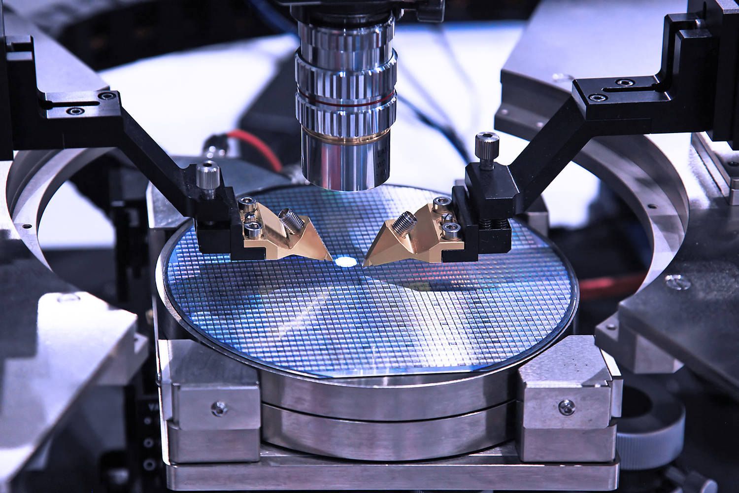
How Bare Wafer Inspection Strengthens Yield Management
Yield—the percentage of functional chips per wafer—is the heartbeat of semiconductor profitability. Any reduction in yield directly affects production cost and output efficiency. Bare wafer inspection contributes to higher yield by identifying minute surface anomalies before patterning begins.
Through techniques such as optical scanning, laser interferometry, and atomic force microscopy, wafer surfaces are analyzed for micro-scratches, pits, and contamination. These inspections are quantified and mapped to track defect trends across batches. Over time, this data helps fabs optimize process recipes, improve cleanroom controls, and correlate defect density with yield metrics.
In short, bare wafer inspection transforms from a simple checkpoint into a strategic data source for continuous improvement.
Ensuring Equipment And Process Integrity
Beyond defect detection, bare wafer inspection also serves as a diagnostic tool for equipment health. Particle contamination may stem not from the wafer itself but from deposition chambers, polishing pads, or even robotic handling systems. Regular inspection provides early warning of tool degradation or contamination leaks.
For high-volume manufacturers, predictive maintenance powered by inspection analytics helps minimize downtime and extend equipment lifespan. This proactive approach not only safeguards yield but also enhances overall operational efficiency—a crucial advantage in a competitive global market where uptime equals profit.
Supporting Next-Generation Semiconductor Technologies
As the industry moves toward smaller nodes and 3D architectures, inspection requirements grow more stringent. Advanced devices such as logic processors and memory chips demand near-zero defect tolerance. Bare wafer inspection evolves alongside these technologies, integrating AI-driven image recognition and advanced metrology systems to detect anomalies that traditional optical tools might miss.
For fabs in Malaysia competing on quality and innovation, mastering this inspection capability is essential. It ensures compliance with global standards while positioning the nation as a trusted partner in the high-tech manufacturing value chain.
The Strategic Value Of Early Defect Control
Investing in robust bare wafer inspection practices yields measurable returns across the production lifecycle. Early defect control minimizes wafer scrap rates, reduces chemical and energy waste, and shortens cycle times. More importantly, it fosters a culture of precision that permeates every downstream process—from lithography to packaging.
When inspection data is integrated with Manufacturing Execution Systems (MES), fabs gain real-time visibility of quality trends, allowing rapid corrective actions. This end-to-end traceability is becoming a benchmark for operational excellence across advanced fabs worldwide.
Conclusion: Precision Begins Before The First Layer
In semiconductor manufacturing, perfection starts long before circuitry is etched. Bare wafer inspection is not a minor procedural step—it is the cornerstone of quality assurance, yield optimization, and process reliability. By identifying imperfections at their source, manufacturers safeguard their investments, strengthen supply chain credibility, and accelerate time-to-market for next-generation devices.
As the semiconductor sector in Malaysia continues to expand, embracing rigorous bare wafer inspection standards will be key to sustaining competitiveness and delivering world-class performance in an industry defined by precision.